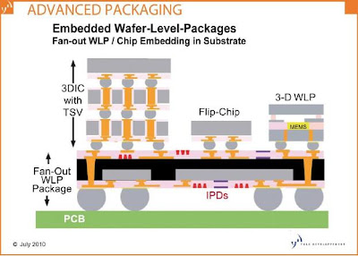
Historically, embedded IC package technology is not new at all: several players such as Freescale with its RCP, Infineon with its eWLB and Ibiden for die embedding into PCB laminated substrates have developed dedicated technologies and process IP in this area for years. Benefits of embedded package integration include miniaturization, improvement of electrical and thermal performance, cost reduction and sim-plification of logistic for OEMs.
“Things are moving really fast at the moment as this year, we see both Fan-out wafer level packaging and chip embedding into PCB laminate infrastructures emerging at the same time, ramping to high volume production," says J. Baron, Technology & Marketing Analyst at Yole Développement.
 Source: Yole Développement, France.
Fan-Out WLP technology emerging on both 200mm/300mm infrastructures
Infineon is having a great success with its proprietary eWLB technology: the first FO-WLP wafers are mass produced on 200mm both at Infineon, STATS ChipPAC and ASE since 2009.
Indeed, Fan-Out WLP is extending the general concept of Wafer Scale Packaging to new application categories, especially the ones with higher pin-counts and larger chip size such as wireless communication ICs. First embedded package products based on eWLB have been identified within LGE and Nokia handsets.
This year, a few additional players are even more aggressive in putting further ca-pacity for eWLB manufacturing as both STATS ChipPAC and NANIUM are at the moment ramping-up their facilities for manufacturing the first generation eWLB on 300mm reconfigured wafers.
Other packaging houses such as SPIL, Amkor, UTAC, ACET and others are also on the point to announce the start of their own Fan-out wafer level packaging operations.
Embedded die package technology to expand fast from niche to high volume markets
Simultaneously, the embedded die package technology has made a lot of progress on its side. Based on PCB laminate infrastructure, chip embeddeding technology is actually on the way to catch a relatively important portion of the actual WLCSP packaging business as it does leverage the existing WLP/RDL infrastructure already established worldwide.
Indeed, most of WLCSP die applications are “embedded ready”, so to realize the full benefits of this “WLCSP to Embedded die” conversion, only a few extra manufacturing steps are missing like the realization of thin copper plating process, extreme wafer thinning down to 50μm, thin dies handling and dicing.
Electrical performance, testing and manufacturing yields are still major issues and showstoppers for chip embedding technology to move forward. Therefore, initial volume markets for embedded packages will be rather small, low pin-counts analog type of applications such as integrated passive devices (IPD), RFID and power com-ponents that are at the moment under qualification for mass production before the end of this year already.
Generally speaking, Yole Développement believe that the winning situation for em-bedded die packages can be met for company partnerships able to cross-over the traditional packaging, assembly and test supply chain.
A good example would be to put together a leading analog IC player (such as TI, Maxim IC, NXP or ST) with a WLP/RDL partner (such as FCI, Casio Micronics, NEPES, etc.) together with a PCB integrator player (such as Imbera/Daeduck, Ibiden, AT&S, Taiyo Yuden or SEMCO).
This type of emerging partnerships are absolutely necessary in order to standardize the embedded package technology and to leverage an entire new packaging infra-structure based on low-cost, panel size PCB manufacturing techniques.
FOWLP vs. chip embedding: Competing technologies and infrastructures?
Today, embedded die and Fan-Out WLP technologies are not competing at all. Indeed, these two emerging semiconductor packaging techniques are targeting very different applications initially: the chip embeddeding technology is looking for re-placement of low cost, low pin-counts WLCSP/SOT/QFN/LGA family package ap-plications while FOWLP technology is rather targeting the direct replacement of higher I/Os (> 120 pins) BGA package applications.
However, in the long term, with standardization and through further technology improvements towards higher yield, better electrical performance, lower profile, better testability and smaller pitch features, fan-out WLP and embedded die technology could seriously compete in the fast growing 3D packaging market space as they will both enable the construction of ever more complex, larger SiP modules with different active and passive functions, all connected on both sides of the active substrate.
So, fan-out WLP and chip embeddeding into PCB laminates are just two additional key pieces of the widening tool-box for 3D packaging!

No comments:
Post a Comment
Note: Only a member of this blog may post a comment.